Aditya Jalkote (@rideraj3) 's Twitter Profile
Aditya Jalkote

@rideraj3

"Electronics Engineer | Passionate about hardware projects, VLSI, and PCB design | ViT'25🎓| Editor - cinematography 📸🎥 | 🇮🇳 | Passion meets innovation🔧|

ID: 1158897891597070339

linkhttps://youtube.com/channel/UCuDNdqdK8FF-Jz0bTWcrOFQ calendar_today07-08-2019 00:29:23

37 Tweet

47 Takipçi

56 Takip Edilen

Aditya Jalkote (@rideraj3) 's Twitter Profile Photo

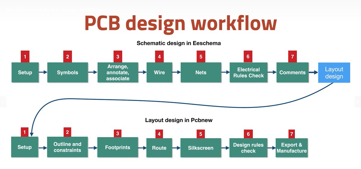
📅 **Day 2: PCB Design Journey Continues!** - schematic and PCB design workflow 💡📟 - Learned to start Eeschema and set up a sheet 🛠️ - Performed an Electrical Rules Check (ERC) with Design✅ Led Torch As First Project excited to see 🌟 #PCBDesign #KiCad #ElectronicsLearning

📅 **Day 2: PCB Design Journey Continues!**

- schematic and PCB design workflow 💡📟
- Learned to start Eeschema and set up a sheet 🛠️
- Performed an Electrical Rules Check (ERC) with Design✅
Led Torch As First Project excited to see 🌟  
#PCBDesign #KiCad #ElectronicsLearning
Aditya Jalkote (@rideraj3) 's Twitter Profile Photo

🚀 Calling all hardware enthusiasts! 🔧 Into KiCad, VLSI, #PCB design, or electronics? 💡 Let’s connect, share ideas, collaborate on exciting projects. 👇 Drop a comment or DM if you're interested! #HardwareTech #ElectronicsEngineering #VLSI #KiCad #semiconductor #ECE

🚀 Calling all hardware enthusiasts!  
🔧 Into KiCad, VLSI, #PCB  design, or electronics?  
💡 Let’s connect, share ideas,  collaborate on exciting 
projects. 

👇 Drop a comment or DM if you're interested!  
#HardwareTech #ElectronicsEngineering #VLSI #KiCad
#semiconductor #ECE
Aditya Jalkote (@rideraj3) 's Twitter Profile Photo

📅 Day 3: Progressing with PCB Design! Designed my first #PCB an LED Torch!💡 -Learned to add components -connect circuits 🛠️ - Routed the board and checked design rules✅ - Visualized the final design in 3D🔍 Excited to see #🚀 #ElectronicsLearning #PCBDesign #KiCad

Aditya Jalkote (@rideraj3) 's Twitter Profile Photo

🌟Calling All Hardware Enthusiasts 🔧 #Hardware Development ⚡ #PCB Design (#KiCAD, Altium, Eagle) 📡 #IoT & #Embedded Sys 🔋 #PowerElectronics & #VLSI 📟 #Microcontrollers Let’s connect, collaborate! DM me😊! #HardwareDesign #semiconductor #ElectronicsEngineering #ECE #EEE

Aditya Jalkote (@rideraj3) 's Twitter Profile Photo

📅Day 4: Advancing in #PCBDesign Setup the board Defined board outline and constraints 🖼️ Placed footprints Routed traces🔗 Added silkscreen 🎨 Performed Design Rules Check✅ Excited to design the life! 🌟 #semiconductor #KiCad #ElectronicsLearning

Aditya Jalkote (@rideraj3) 's Twitter Profile Photo

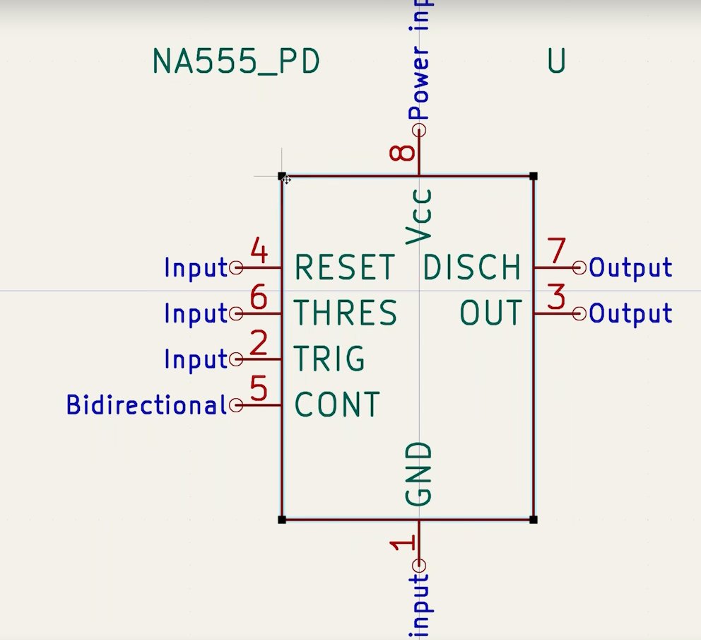
📅 Day 5: Deep Dive into #PCBDesign! 💡 Designed my first IC schematic: the #555Timer #IC Got help from a #TexasInstruments datasheet for symbol and footprint. - Learned to find and install symbols📚 - Created custom symbols and linked footprints✏️ #KiCad #Electronics

📅 Day 5: Deep Dive into #PCBDesign!

💡 Designed my first IC schematic: the #555Timer #IC  
Got help from a #TexasInstruments datasheet for symbol and footprint.    

- Learned to find and install symbols📚  
- Created custom symbols and linked footprints✏️
 #KiCad #Electronics
Aditya Jalkote (@rideraj3) 's Twitter Profile Photo

📅 Day 6: Fundamentals and Review Revised concepts for a stronger foundation 📖✅ Explored editor preferences, board setup, and design rules 🛠️ Worked with zones, keep-outs, and interactive routing 🔗 Feeling confident with PCB design basics! 🚀 #PCBDesign #KiCad #Electronics

Aditya Jalkote (@rideraj3) 's Twitter Profile Photo

📅Day 7: Custom #Footprints and #Gerber Files -Learned to create custom footprints -Fabrication layer🛠️ -Pads -Courtyard layer -Silkscreen layer🎨 -Found and used 3D shapes for footprints🔍 -Exported and tested Gerber files for manufacturing✅ #PCBDesign #KiCad

Aditya Jalkote (@rideraj3) 's Twitter Profile Photo

📅Day 8 Past week, I’ve made progress in learning #PCBdesign, building base and understood the basics , My interest in PCB design has grown, and I feel more confident. Tomorrow, will start a new #PCB project , I hope this journey will improve my knowledge, help in future.

📅Day 8

Past week, I’ve made  progress in learning 
#PCBdesign, building base and understood the basics , My interest in PCB design has grown, and I feel more confident. 

Tomorrow, will start a new #PCB project , I hope this journey will improve my knowledge, help in  future.
Aditya Jalkote (@rideraj3) 's Twitter Profile Photo

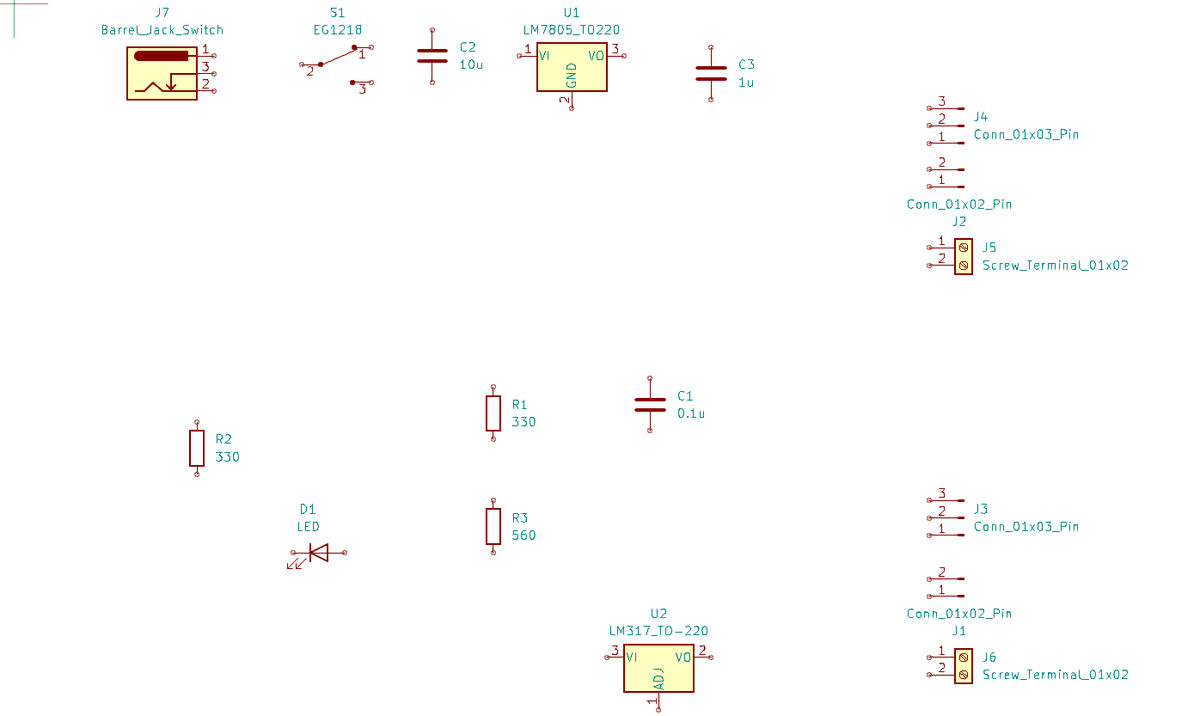
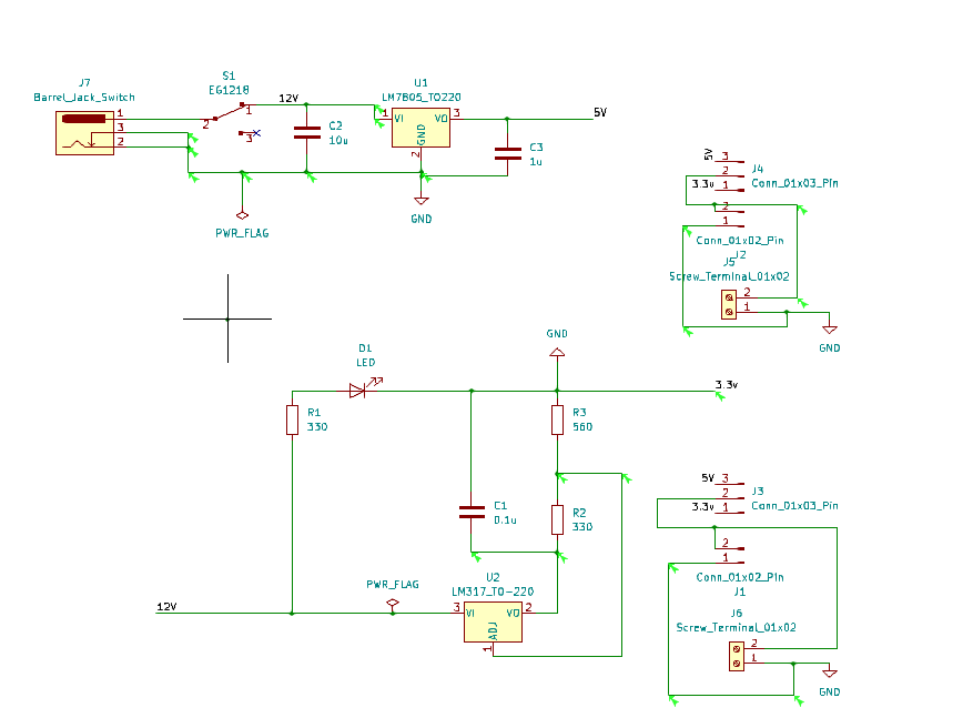
📅Day 9~ #New_project to design a #power supply PCB for a #breadboard 🛠️🚀 - Set up the schematic and added symbols for components 📐 - Wired the circuit and created nets 🔌 - Performed (#ERC) ✅ - Added comments for clarity ✏️ #PCBDesign #KiCad #Electronics #vlsi

Aditya Jalkote (@rideraj3) 's Twitter Profile Photo

📅Day 10: Progressing Work on the power supply #PCBdesign project is ongoing and taking shape 🛠️. - Reviewed the schematic setup, symbols, and wiring from Day 9🔌 - Preparing for layout design and ensuring all fundamentals are solid 📐 #Embeded #KiCad #Electronics #vlsi

Aditya Jalkote (@rideraj3) 's Twitter Profile Photo

📅Day 11: Project + DMM Basics - Progressed on the power supply PCB design 🛠️ - Digital Multimeter (DMM) usage: tested components like fuses, batteries, capacitors, resistors, transistors, and ICs 🔍 Boosting skills in testing electronics! 🚀 #PCBDesign #DMM #Electronics

Aditya Jalkote (@rideraj3) 's Twitter Profile Photo

📅Day 12: A Quiet Day Not feeling well today 🤒, so progress was minimal. Spent some time exploring internship and job opportunities on LinkedIn 💼. Hoping to bounce back stronger tomorrow! 💪 #PCBDesign #JobHunting #Electronics #VLSI #Embeded #Kicad #HardwareEnineer #JOB

Aditya Jalkote (@rideraj3) 's Twitter Profile Photo

📅 Day 13: #Progress Update Faced a slight delay in the #project but made progress on designing a suitable #PCB layout. Working on optimizing the board to fit properly while refining the schematic connections. Keeping the momentum going🚀 #PCBDesign #HardwareTech #VLSI #KiCad

📅 Day 13: #Progress Update

Faced a slight delay in the #project but made progress on designing a suitable #PCB layout. Working on optimizing the board to fit properly while refining the schematic connections. Keeping the momentum going🚀

#PCBDesign #HardwareTech  #VLSI #KiCad
Aditya Jalkote (@rideraj3) 's Twitter Profile Photo

📅 Day 14: Worked on identifying and correcting a design defect in the schematic and layout. 🛠️ Focused on improving the design with proper fixes. ✅ 🎯 Next Goal: Complete the PCB project in the next 2-3 days! 🚀 #PCBDesign #HardwareTech #VLSI #KiCad #ElectronicsEngineering

📅 Day 14:

Worked on identifying and correcting a design defect in the schematic and layout. 🛠️

Focused on improving the design with proper fixes. ✅

🎯 Next Goal: Complete the PCB project in the next 2-3 days! 🚀

#PCBDesign #HardwareTech #VLSI #KiCad
#ElectronicsEngineering
Aditya Jalkote (@rideraj3) 's Twitter Profile Photo

📅 Day 15 Update- Completed wire connections and schematic design ✅ Passed the Electrical Rules Check (ERC) 🛠️ Added footprints to all symbols for PCB layout 🌟 Steady progress on the project! 🚀 #PCBDesign #KiCad #Electronics #VLSI #Progress #UPDATE #engineering #Passion

📅 Day 15 Update-

Completed wire connections and schematic design ✅

Passed the Electrical Rules Check (ERC) 🛠️

Added footprints to all symbols for PCB layout 🌟

Steady progress on the project! 🚀 
#PCBDesign #KiCad #Electronics #VLSI
#Progress #UPDATE #engineering #Passion
Aditya Jalkote (@rideraj3) 's Twitter Profile Photo

Day 16: Kind Of Skip Day Not feeling well today, so I couldn’t do much. Hoping to recover soon and continue the journey. Meanwhile, exploring platforms for jobs and internships. #Pcbdesign #vlsi #learning #internship #kicad #Altium #eagle #embeded #electronics #Semiconductots