ChipIN Centre (@chipin_goi) 's Twitter Profile
ChipIN Centre

@chipin_goi

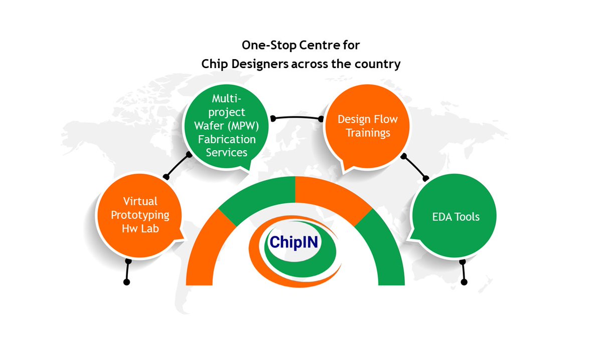
One-stop Centre for Chip designers across the country:
1. EDA Tools
2. MPW fab
3. Design training
4. Post-Si validation
Details at c2s.gov.in/chipin.jsp

ID: 1654398790990958592

linkhttps://chips-dli.gov.in/ calendar_today05-05-2023 08:13:19

16 Tweet

232 Takipçi

14 Takip Edilen

C-DAC Bengaluru (@cdacbengaluru) 's Twitter Profile Photo

MoS Rajeev Chandrasekhar (Parody) announces ChipIN Centre at C-DAC India Bangalore; which will act as one stop centre to provide #Semiconductor Design Tools, Fab access, Virtual Prototyping Hw Lab access to Fabless Chip Designers of the country. #SemiconIndia IISc Bangalore
MoS <a href="/Rajeev_GoI/">Rajeev Chandrasekhar (Parody)</a> announces ChipIN Centre at 
<a href="/cdacindia/">C-DAC India</a> Bangalore; which will act as one stop centre to provide #Semiconductor Design Tools, Fab access, Virtual Prototyping Hw Lab access to Fabless Chip Designers of the country. #SemiconIndia 
<a href="/iiscbangalore/">IISc Bangalore</a>
Rajeev Chandrasekhar 🇮🇳 (@rajeevrc_x) 's Twitter Profile Photo

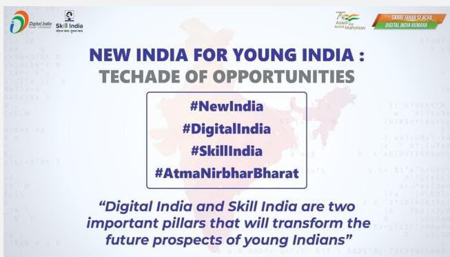
Time to be a India Semiconductor Mission #futureDESIGN #startup is now! PM Narendra Modi ji is propelling #NewIndia n YoungIndians into Techade of Opportunities. Be a part of #SemiconIndia futureDESIGN Roadshow at IIT Delhi on 12th May 2023 aimed at catalyzing next-gen #Semiconductor

Time to be a <a href="/Semicon_India/">India Semiconductor Mission</a>  #futureDESIGN #startup is now!

PM <a href="/narendramodi/">Narendra Modi</a> ji is propelling #NewIndia n YoungIndians into Techade of Opportunities. 

Be a part of #SemiconIndia futureDESIGN Roadshow at <a href="/iitdelhi/">IIT Delhi</a> on 12th May 2023 aimed at catalyzing next-gen #Semiconductor
Rajeev Chandrasekhar 🇮🇳 (@rajeevrc_x) 's Twitter Profile Photo

India’s one-stop centre for chip design & fabrication is here! ChipIN Centre setup at C-DAC India, will provide chip design & fabrication support & services to fabless chip designers in the country, which includes: ➡️ Fab Multi-project Wafer (MPW) services at Semi-Conductor Laboratory and
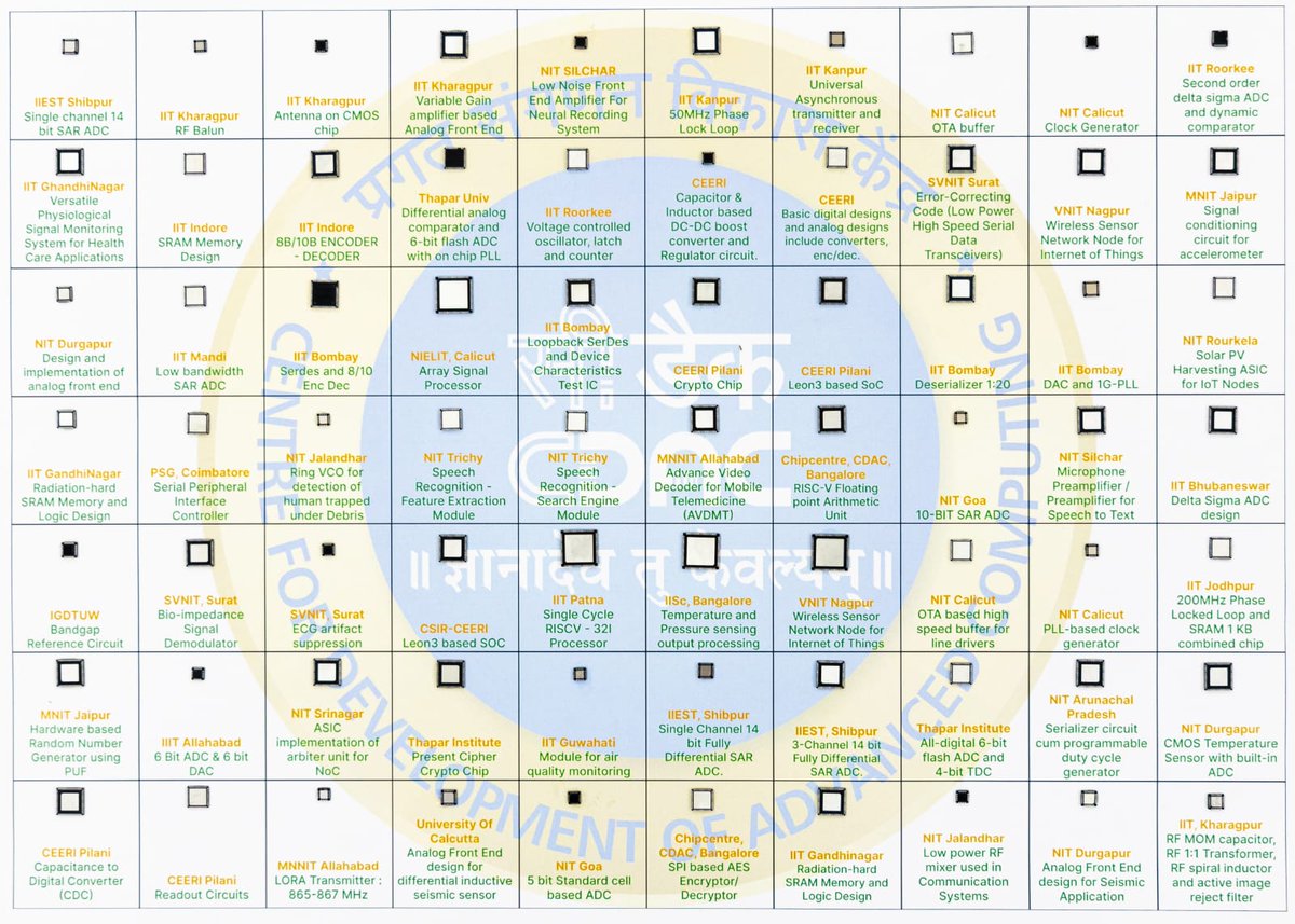
India’s one-stop centre for chip design &amp; fabrication is here!

<a href="/ChipIN_GoI/">ChipIN Centre</a> setup at <a href="/cdacindia/">C-DAC India</a>, will provide chip design &amp; fabrication support &amp; services to fabless chip designers in the country, which includes:

➡️ Fab Multi-project Wafer (MPW) services at <a href="/SclMohali/">Semi-Conductor Laboratory</a> and
Aashish Chandorkar (@c_aashish) 's Twitter Profile Photo

ChipIN Centre at C-DAC Bangalore will act as one-stop centre to provide semiconductor design tools, fab access, virtual prototyping hardware lab access to fabless chip designers from Startups and Academia. It is a common dedicated centralised cloud-supported design facility, not

Digital India (@_digitalindia) 's Twitter Profile Photo

.ChipIN Centre setup as a one-stop center at C-DAC India for meeting the semiconductor design and fabrication needs of the Indian fabless designers. #ChipINInsights shared with 250 chip designers under the Chips to Start-up (C2S) Programme for making use of Synopsys leading-edge
.<a href="/ChipIN_GoI/">ChipIN Centre</a> setup as a one-stop center at <a href="/cdacindia/">C-DAC India</a> for meeting the semiconductor design and fabrication needs of the Indian fabless designers.

#ChipINInsights shared with 250 chip designers under the Chips to Start-up (C2S) Programme for making use of <a href="/Synopsys/">Synopsys</a> leading-edge
Digital India (@_digitalindia) 's Twitter Profile Photo

🚀 Design Semiconductor Chips in India 🇮🇳, for the World 🌏 ☑️ ChipIN Centre invites #Semi Chip designers across India - Academia and Start-ups/ MSMEs to access the National EDA Tool Grid & other resources ☑️ Eligible academia and Start-ups to register for #Semi Chip design

🚀 Design Semiconductor Chips in India 🇮🇳, for the World 🌏

☑️ <a href="/ChipIN_GoI/">ChipIN Centre</a> invites #Semi Chip designers across India - Academia and Start-ups/ MSMEs to access the National EDA Tool Grid &amp; other resources

☑️ Eligible academia and Start-ups to register for #Semi Chip design
Digital India (@_digitalindia) 's Twitter Profile Photo

📢 ChipIN Centre 🇮🇳 invites for hands-on training on Analog Mixed-Signal #AMS using EDA tools from Synopsys from June 24-28, 2024 🎯 All students, researchers & faculty members from 150 organizations under Chips to Start-up #C2S Programme are eligible to attend. 🌐 Contact

📢 <a href="/ChipIN_GoI/">ChipIN Centre</a> 🇮🇳 invites for hands-on training on Analog Mixed-Signal #AMS using EDA tools from <a href="/Synopsys/">Synopsys</a> from June 24-28, 2024

🎯 All students, researchers &amp; faculty members from 150 organizations under Chips to Start-up #C2S Programme are eligible to attend.

🌐 Contact
Digital India (@_digitalindia) 's Twitter Profile Photo

📢@ChipIN Centre 🇮🇳 announces MPW (Multi-project Wafer) Shuttle-I for fabrication of designs by 113 organizations under C2S (Chips to Start-up) Programme at 180nm, SCL (Semi-Conductor Laboratory) Mohali. For details, please visit c2s.gov.in/SCL_MPW.jsp #ChipsforViksitBharat

📢@ChipIN Centre 🇮🇳  announces MPW (Multi-project Wafer) Shuttle-I for fabrication of designs by 113 organizations under C2S (Chips to Start-up) Programme at 180nm, SCL (Semi-Conductor Laboratory) Mohali. For details, please visit c2s.gov.in/SCL_MPW.jsp
#ChipsforViksitBharat
Digital India (@_digitalindia) 's Twitter Profile Photo

📢 Kickstart your SoC design journey with silicon-proven #IP Cores from Synopsys now made available by ChipIN Centre 🇮🇳 for domestic Start-ups and MSMEs under the #DLI Scheme! 🚀 Don't miss the chance to accelerate your SoC design's time-to-market with silicon-proven Interface

📢 Kickstart your SoC design journey with silicon-proven #IP Cores from <a href="/Synopsys/">Synopsys</a> now made available by <a href="/ChipIN_GoI/">ChipIN Centre</a> 🇮🇳 for domestic Start-ups and MSMEs under the #DLI Scheme!
🚀 Don't miss the chance to accelerate your SoC design's time-to-market with silicon-proven Interface
Digital India (@_digitalindia) 's Twitter Profile Photo

📢 Design Linked Incentive (DLI) Scheme invites proposals from domestic start-ups/ MSMEs for Module Design in identified areas of Wireless and IoT. 🚀 For support on other resources under DLI Scheme, please apply now at chips-dli.gov.in #ChipsforViksitBharat

📢 Design Linked Incentive (DLI) Scheme invites proposals from domestic start-ups/ MSMEs for Module Design in identified areas of Wireless and IoT.
   
🚀 For support on other resources under DLI Scheme, please apply now at chips-dli.gov.in
   
#ChipsforViksitBharat
Digital India (@_digitalindia) 's Twitter Profile Photo

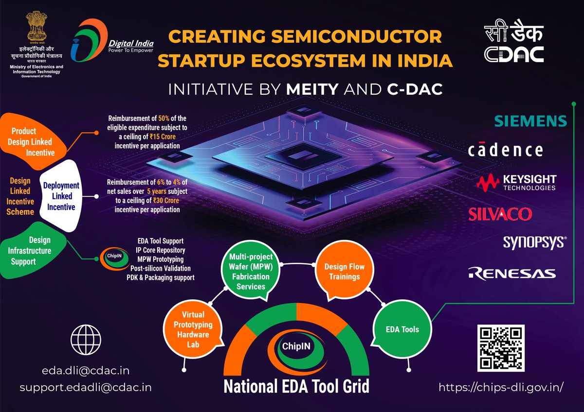
📢 #DLI (Design Linked Incentive) Scheme & #C2S (Chips to Start-up) Programme invites domestic designers to avail the National Fabless Chip Design Infrastructure at ChipIN Centre ✅ EDA Tools: Synopsys, Cadence Design Systems, Siemens EDA, Keysight Technologies, SILVACO, Ansys,

📢 #DLI (Design Linked Incentive) Scheme &amp; #C2S (Chips to Start-up) Programme invites domestic designers to avail the National Fabless Chip Design Infrastructure at ChipIN Centre

✅ EDA Tools: Synopsys, Cadence Design Systems, Siemens EDA, Keysight Technologies, SILVACO, Ansys,
PIB India (@pib_india) 's Twitter Profile Photo

💠Government of India creating enabling environment for Semiconductor Design Community with direct access to National Chip Design Infrastructure 💠ChipIN (CDAC), one-stop centre for chip designers nationwide, gets momentum with extended support from semiconductor industry leader

💠Government of India creating enabling environment for Semiconductor Design Community with direct access to National Chip Design Infrastructure

💠ChipIN (CDAC), one-stop centre for chip designers nationwide, gets momentum with extended support from semiconductor industry leader
India Semiconductor Mission (@semicon_india) 's Twitter Profile Photo

📢ChipIN Centre 🇮🇳 invites students, faculty members & engineers from 300 organizations supported under #C2S Programme and #DLI Scheme for training on solutions from Keysight Technologies, ANSYS, XILINX (AMD) and IPR. 🌐More details at c2s.gov.in/EDA_Tool_Suppo… #ISM #SemiconIndia
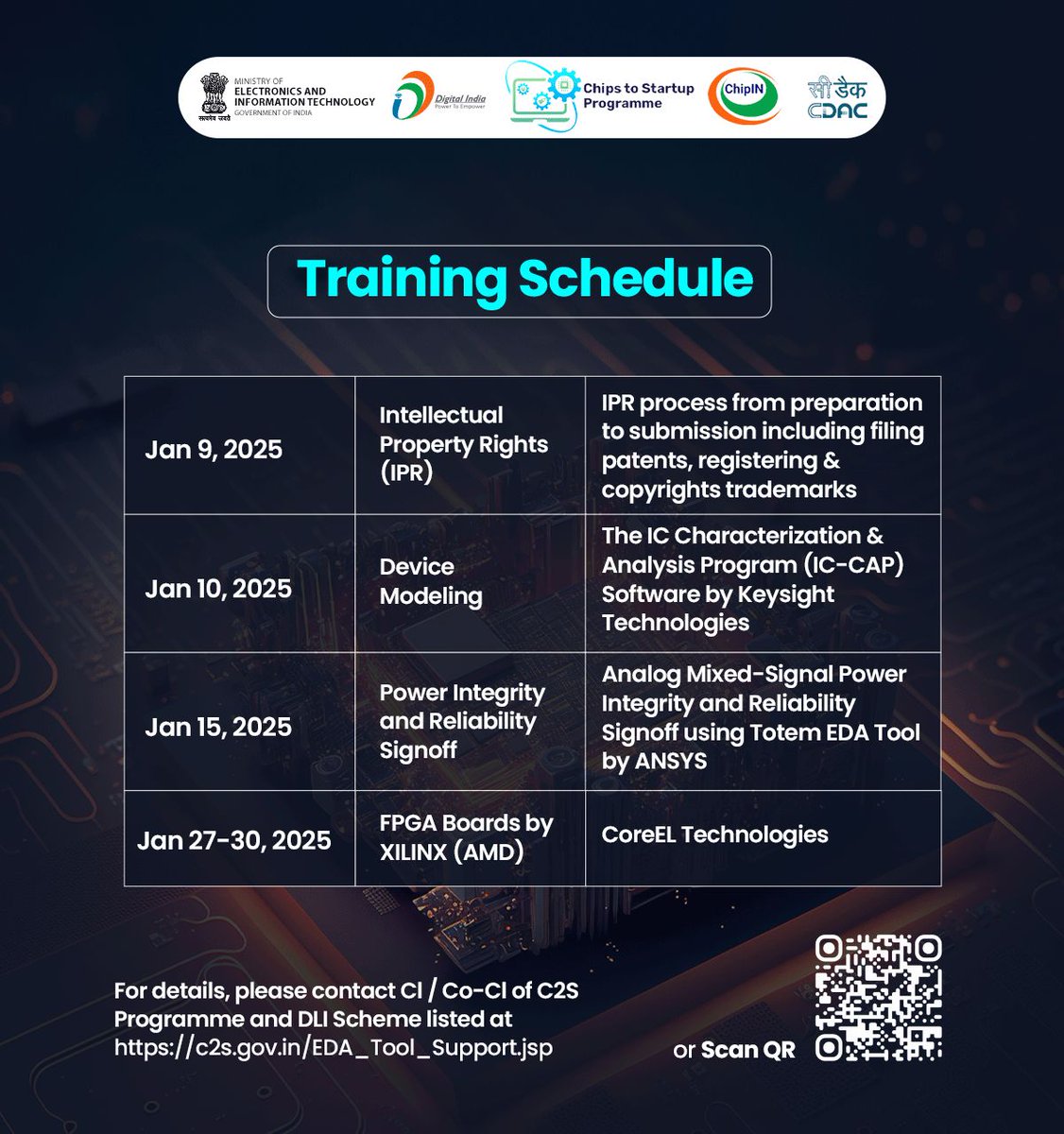
📢<a href="/ChipIN_GoI/">ChipIN Centre</a> 🇮🇳 invites students, faculty members &amp; engineers from 300 organizations supported under #C2S Programme and #DLI Scheme for training on solutions from Keysight Technologies, ANSYS, XILINX (AMD) and IPR.  

🌐More details at c2s.gov.in/EDA_Tool_Suppo…

#ISM #SemiconIndia