Matthew Hartensveld, PhD
@matthartensveld
Posts related to homebrew semiconductor device fabrication and
semiconductor news.
ID: 2320180861
http://matt.engineer 31-01-2014 03:49:00
24 Tweet
33 Followers
55 Following
 on Twitter photo Homebrew spin coater. Programmable RPM with hall sensor, use of hdd motor, ardunio, mini air pump, and quad copter driver board.")
 on Twitter photo Microscope lithography with infinity correction. Use of mylar mask in place of polarizer. Looks like it should be possible to get sub-micron features, though with a small field size. The spectrometer is used for film thickness measurements.")
 on Twitter photo Modified HP4145A semiconductor parameter analyzer with basic probe station. Results were from testing an homemade diode made back in high school.")
 on Twitter photo Got interested in AI and how it can be applied to semiconductor research. I have generated over 36,000 QA pairs on my notes, papers saved, and lectures transcribed, of which I used LoRA to finetune a Mistral model. Happy with the initial results, with plans to expand it.")
 's Twitter Profile Photo")
 on Twitter photo Sputter gun assembled!")
 on Twitter photo New chamber \"hat\" to make room for the sputter gun")
 on Twitter photo Automation in progress + sub 100nm features?")
 on Twitter photo Assembling the sputter coater")
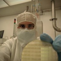
 on Twitter photo")
@matthartensveld
Posts related to homebrew semiconductor device fabrication and
semiconductor news.
ID: 2320180861
http://matt.engineer 31-01-2014 03:49:00
24 Tweet
33 Followers
55 Following