Nanosurf(@NanosurfAFM) 's Twitter Profileg
Nanosurf

@NanosurfAFM

Nanosurf was founded in 1997 in Liestal, Switzerland, and has since become one of the most highly trusted atomic force microscopy brands in existence.

ID:3392111734

linkhttp://www.nanosurf.com calendar_today28-07-2015 13:47:37

552 Tweets

790 Followers

193 Following

Nanosurf(@NanosurfAFM) 's Twitter Profile Photo

This application note demonstrates, through examples, how to use Spectroscopy Plus on the DriveAFM to setup complex experiments and investigate cell mechanics.


hubs.ly/Q02vQ-V80

account_circle
Nanosurf(@NanosurfAFM) 's Twitter Profile Photo

This technical note explores the use of Scanning Microwave Microscopy in the semiconductor industry as an essential technique for examining the electrical characteristics of semiconductors with high precision and sensitivity.
hubs.la/Q02v63xQ0

account_circle
Nanosurf(@NanosurfAFM) 's Twitter Profile Photo

, the first commercial photothermal off-resonance tapping mode was launched in February 2022. Learn from our experts about the benefits of WaveMode, when it is most beneficial, and what to look out for.
hubs.la/Q02mnlh90

account_circle
Nanosurf(@NanosurfAFM) 's Twitter Profile Photo

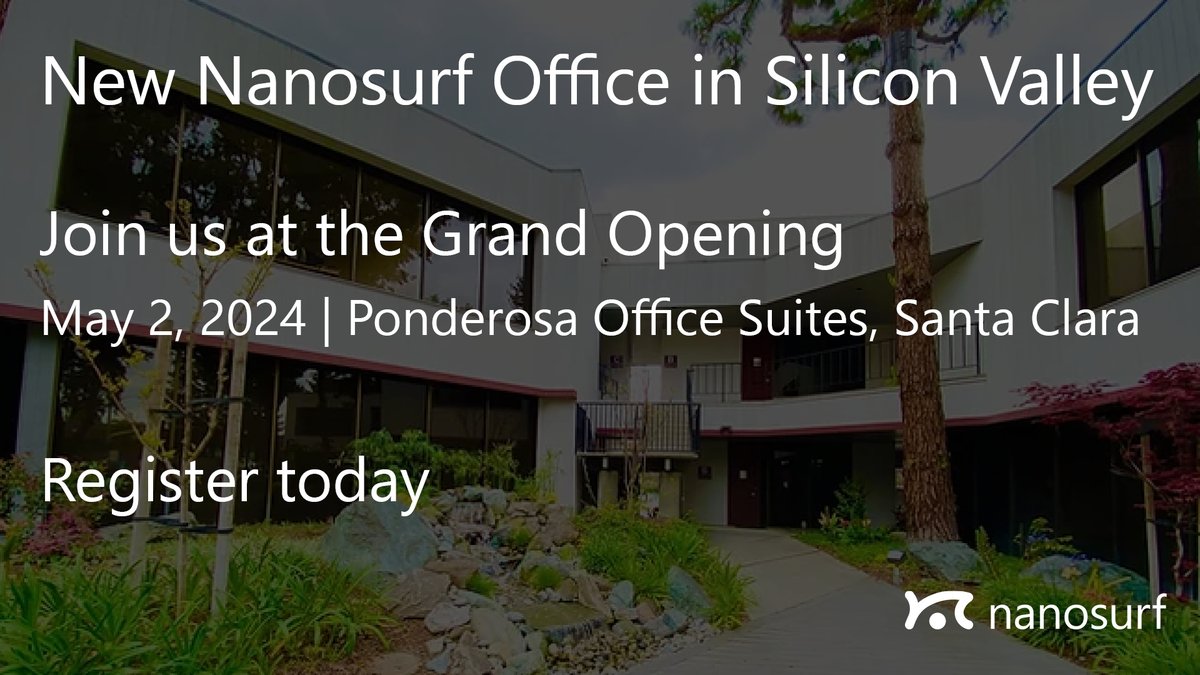
We are thrilled to announce the grand opening of Nanosurf's new office in the heart of Silicon Valley, and look forward to celebrating with our partners, clients, and friends. Join our Opening Reception and celebrate with us on May 2nd, 2024.
hubs.la/Q02tTtyL0

We are thrilled to announce the grand opening of Nanosurf's new office in the heart of Silicon Valley, and look forward to celebrating with our partners, clients, and friends. Join our Opening Reception and celebrate with us on May 2nd, 2024. hubs.la/Q02tTtyL0
account_circle
Nanosurf(@NanosurfAFM) 's Twitter Profile Photo

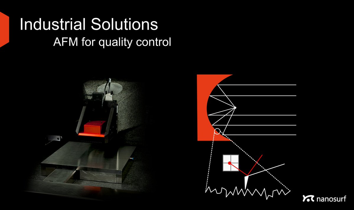
Do you care about surface finish?
Need to comply within certain specifications but no tool can measure the surface quality of your products?
At Nanosurf we have the solution.

Learn about our solutions for industry at
hubs.la/Q02thrW60

Do you care about surface finish? Need to comply within certain specifications but no tool can measure the surface quality of your products? At Nanosurf we have the solution. Learn about our solutions for industry at hubs.la/Q02thrW60 #AFM #roughness #industry #surfaces
account_circle
Nanosurf(@NanosurfAFM) 's Twitter Profile Photo

Probably the most common AFM mode to measure mechanical properties such as modulus and adhesion is spectroscopy. This session discusses what a force curve measures and the different models available for force curve analysis.
hubs.la/Q02mncKk0

account_circle
Nanosurf(@NanosurfAFM) 's Twitter Profile Photo

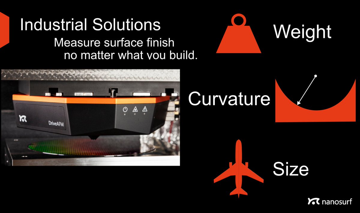
Care about surface finish, but your product is very heavy, has a high curvature, or simply it is too large?
At Nanosurf we deal with all of these problems to bring you the results your need.

hubs.la/Q02syTt80

Care about surface finish, but your product is very heavy, has a high curvature, or simply it is too large? At Nanosurf we deal with all of these problems to bring you the results your need. hubs.la/Q02syTt80 #AFM #roughness #industry #surfaces
account_circle
Nanosurf(@NanosurfAFM) 's Twitter Profile Photo

For certain quantitative measurements, calibrations of key AFM parameters such as cantilever spring constant and sensitivity are critical. This AFM Master Class session reviews the different methodologies for conducting the various calibrations.

hubs.la/Q02mnjXr0

account_circle
Nanosurf(@NanosurfAFM) 's Twitter Profile Photo

Are you an expert on processing AFM images?
If not, this AFM Master Class session will be useful to you. You will learn about basic image processing steps as well as some additional useful image processing such as histograms, 3-D overlays, and masking.
hubs.la/Q02mnk6l0

account_circle
Nanosurf(@NanosurfAFM) 's Twitter Profile Photo

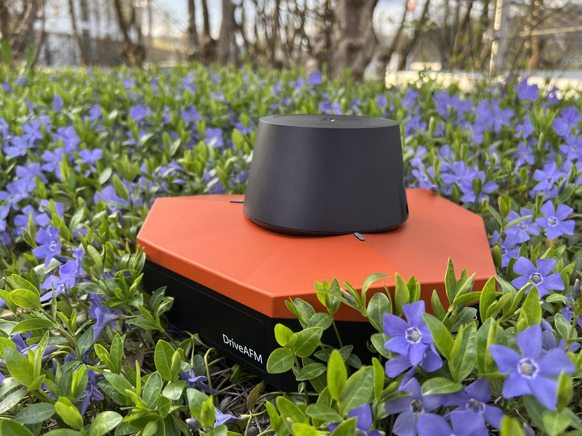
Happy Easter! Wishing a beautiful spring weekend to all our colleagues and friends. This sets a good example - take the opportunity to get outside and bask in the abundant natural beauty of the season.

Happy Easter! Wishing a beautiful spring weekend to all our colleagues and friends. This #DriveAFM sets a good example - take the opportunity to get outside and bask in the abundant natural beauty of the season.
account_circle
Nanosurf(@NanosurfAFM) 's Twitter Profile Photo

Learn about Nanoelectrical Characterization in Nanosurf's AFM Master Class. This session covers the key AFM modes to measure a variety of electrical properties including surface potential, piezoelectric properties and conductivity.

hubs.la/Q02mnjNT0

account_circle
Nanosurf(@NanosurfAFM) 's Twitter Profile Photo

Discover how Federico Colombo and colleagues used a FlexAFM to track the mass of individual cells. Read about their publication to find out why Nanosurf is a brand that researchers can confidently recommend for AFM solutions.

hubs.la/Q02p_p500

Discover how Federico Colombo and colleagues used a FlexAFM to track the mass of individual cells. Read about their publication to find out why Nanosurf is a brand that researchers can confidently recommend for AFM solutions. #cellbio #AFM #article hubs.la/Q02p_p500
account_circle
Nanosurf(@NanosurfAFM) 's Twitter Profile Photo

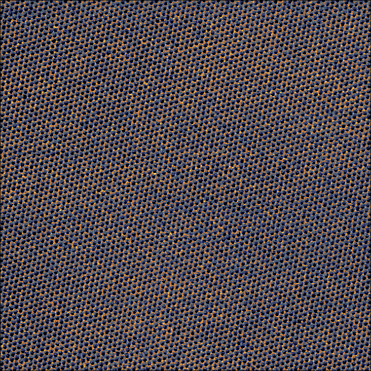
This photothermal torsional resonance image of hexagonal boron nitride (hBN) layer on graphene captures a moiré superlattice pattern, with a subtle 2.2° twist between the layers. (image size: 500 nm; color scale: 9.6°)
Learn more: hubs.la/Q02mq9f70

This photothermal torsional resonance image of hexagonal boron nitride (hBN) layer on graphene captures a moiré superlattice pattern, with a subtle 2.2° twist between the layers. (image size: 500 nm; color scale: 9.6°) Learn more: hubs.la/Q02mq9f70
account_circle
Nanosurf(@NanosurfAFM) 's Twitter Profile Photo

AFM Master Class on Youtube: This session includes a discussion of what it is exactly that the phase measures, and how it is useful, both as an imaging mode and as an important indicator for topographic imaging.
hubs.la/Q02mn9Vf0

account_circle
Nanosurf(@NanosurfAFM) 's Twitter Profile Photo

This application note explores the use of Atomic Force Microscopy for in-depth analysis of graphene, highlighting its atomic-scale resolution and multifunctional capabilities in characterizing this remarkable 2D material.
hubs.la/Q02mq8jW0

account_circle